

Made in Albany: How an Undergrad, Researcher and Intern Became a Chip Developer at IBM
ALBANY, N.Y. (Feb. 18, 2026) — Belle Antonovich’s first job after earning a bachelor’s in nanoscale engineering — at IBM — was in the same place where she studied and conducted research as an undergraduate student: the NY Creates Albany NanoTech Complex.
That’s because the R&D complex is home to both higher education — specifically the Department of Nanoscale Science & Engineering in UAlbany’s College of Nanotechnology, Science, and Engineering (CNSE) — and industry, including IBM. It’s also because Antonovich interned at Big Blue as an undergrad before graduating in 2022. Yes, impactful classes and internships often spark job offers — just not usually in the same building!
Today, Antonovich is creating the next generation of chips that fuel the global semiconductor industry as a lithography hardware developer. She took a break from her fast-paced role to reflect on her journey.
What do you love about your job?
The sense of accomplishment. I’m fortunate to work on highly impactful projects that contribute to the future of technology. The significance of this work became especially clear when I met with a CEO who collaborates directly with world leaders on planning future fab development. Working in a specialized industry like semiconductors also allows you to shape your own career path and focus on what you truly enjoy. For me, that passion is metrology, specifically CD-SEM. The sense of accomplishment I get from successfully completing a challenging measurement recipe is truly unmatched.
You discovered CNSE in high school during a visit to the NY Creates Albany NanoTech Complex. What stood out?
When I first visited CNSE, it was immediately clear that the program offered a direct pathway into a thriving industry. At the time, the two available majors were specifically designed to prepare students to transition straight into the workforce or an advanced degree. In addition, the abundance of internships was a major selling point. CNSE students are highly competitive candidates for these positions, which are essential for building experience, strengthening your resume and opening doors to career opportunities or graduate programs.
You worked in a lab in your first year. How valuable was that?
Joining a research lab as early as possible is one of the most valuable decisions a student can make. The hands-on experience I gained not only strengthened my technical skills but also played a significant role in helping me secure internships and eventually a full-time position. My research in Dr. (Gregory) Denbeaux’s lab on photoresist chemistry and the optimization of spin‑coating environments is still very relevant to my job role today.
What are the pluses of learning your discipline in an R&D complex?
Being surrounded by active industry professionals is one of the unique advantages of CNSE. Passing engineers in the halls, many of whom could become future colleagues or employers, creates constant opportunities for connection. For example, one of my coworkers even secured an internship simply by starting a conversation with an employee in the parking lot.
Which professors had a lasting impact on you?
Dr. Denbeaux, for the excellent research experiences I gained in his lab. The knowledge and hands‑on skills I developed both through SURP and our SRC‑sponsored project continue to be directly relevant to my work today. Those opportunities played a significant role in shaping my career path, and I am truly grateful for his mentorship, guidance and support.
Who else?
Dr. (Kathleen) Dunn. Her courses are not only highly informative and aligned with industry needs, but her enthusiasm, kindness and ability to make complex topics exciting set her apart as an exceptional educator. I have continued to stay in contact with her, as she is an active member of the semiconductor community, for example, as a panelist and member of WiS (Women in Semiconductors). “In a field of horses, be a unicorn” is my favorite and most memorable quote from Dr. Dunn!
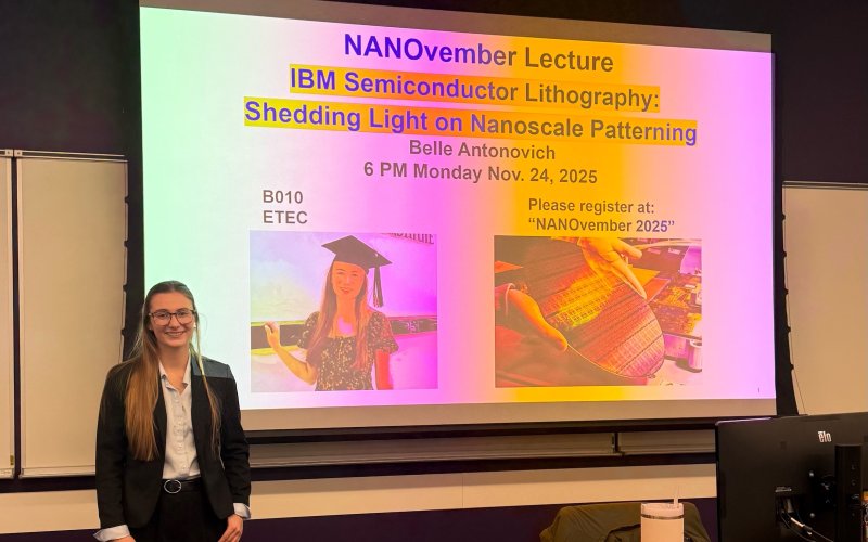
At your NANOvember talk, you acknowledged that nano engineering is challenging and encouraged students to keep going. What kept you going?
Balancing demanding coursework alongside research responsibilities and the pressure of securing internships or job opportunities can be overwhelming. What kept me motivated was knowing that once I secured my first role in the industry, the path ahead would become more manageable and filled with opportunities. A fellow student once told me, “If you work hard for four years during undergrad, you set yourself up for forty years of success in your career.” That perspective stayed with me throughout my undergraduate experience and helped guide me through the toughest moments.
You personify 'brain gain' in New York, as you studied in Albany and now work there. What's the market for your skills here?
New York is an excellent place for anyone with semiconductor skills or experience to build a career. Many of my colleagues have relocated from across the United States or even from overseas specifically to work at the Albany NanoTech Complex. The state has many semiconductor organizations, including IBM, Tokyo Electron Limited, ASML, other tool and materials suppliers at NY Creates, GlobalFoundries in Malta and Wolfspeed in Utica. Engineers also have the flexibility to shift their career paths by exploring opportunities at nearby companies such as Regeneron or Curia.