


CNSE is Making Albany a Hub for Photoresist Innovation
This story first appeared in New York State of Discovery, UAlbany's 2026 research magazine.
ALBANY, N.Y. (March 3, 2026) — New York is buying one of the most complex machines ever built to empower researchers in Albany to push the limits of the advanced computer chips needed for artificial intelligence and other technologies.
In one square inch, each of these chips contains billions of features — almost impossibly tiny transistors, resistors, wires and capacitors. Each one is not much wider than a strand of DNA.
The $500 million machine that helps make them is the centerpiece of New York Gov. Kathy Hochul’s landmark investment in the new High NA EUV Lithography Center at the NY Creates Albany NanoTech Complex.
But it’s only part of the story.
Photoresists are also essential to this process, and University at Albany researchers are making New York a global hub for photoresist innovation.
Chip designs are patterned on silicon wafers using a complex series of processes including EUV — or extreme ultraviolet — lithography. These intricate EUV-produced patterns shape the electrical devices and circuits that make up the logic and memory chips powering your smartphone, your car, data centers and AI as we know it today.
You've seen a grainy photograph. My chemistry allows you to get better resolution.
If the High NA EUV tool coming to Albany NanoTech is the camera, photoresists — the thin, light-sensitive chemical coatings on the silicon wafers — are the film. The analogy isn’t perfect, but it underscores an urgent technical challenge facing the $11 billion-a-year EUV lithography industry.
“The resists we have now are a good start, but to get the most out of this remarkable $500 million camera, we need better resist films that give us better resolution,” said Professor Robert Brainard, a chemist at UAlbany’s College of Nanotechnology, Science, and Engineering (CNSE) and the first person in the world to design resists for EUV. “You've seen a grainy photograph. My chemistry allows you to get better resolution.”
Without better photoresists, the decades-long trend of doubling of the number of transistors on computer chips roughly every two years could falter over time.
“You can buy a car now that is much smarter than it was two years ago,” Brainard said. In part, that’s thanks to new resists that require less light and time in the lithography process, allowing companies to produce their chips faster and more cheaply.
“The chemistry is one of the key technologies that allow the computer chip to be smarter, faster, more efficient, and it allows it to be cost effective,” he said. “It's one thing to put a computer in your car, but if that chip is half the cost of your car, you can’t do it.”
‘Always pushing the limits’
The global photoresist industry is projected to more than quadruple over the next half-decade because the race for chips more densely packed with features depends on better resists. So does the sustainability of an AI industry that must figure out how to increase computational power while consuming less energy.
For two decades at CNSE, Brainard and Associate Professor Gregory Denbeaux have worked to help industrial engineers understand which resists are better — and why.
Denbeaux, a physicist, said “companies are always going to push the limits” of making patterns smaller because it’s basic economics. “They’ll have more features per wafer and chip, and they’ll sell their products for more money than their competitors.”
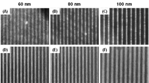
Like many technologies, today’s photoresists were developed through decades of scientific exploration. Chemists like Brainard, who spent 35 years in the industry, continually invented newer resists capable of more intricate patterning using ever-smaller wavelengths of light. Smaller wavelengths enable tighter patterns, leading today to EUV light with wavelengths as small as 13 nanometers (or 13 billionths of a meter).
This meant testing chemical compounds from different parts of the periodic table. Along the way, Brainard pioneered introducing metal compounds into EUV resists to improve their ability to absorb light and trigger the reactions that create nanoscale chip features.
Answering questions no one else can
Why some compounds work better than others is a function of the physics involved when the high-energy EUV light —in the form of photons — hits the photoresists. Denbeaux has developed a global reputation for understanding that part of the process, with help from ERIC.
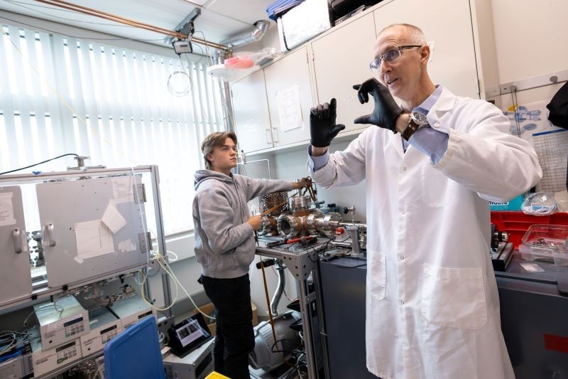
ERIC is the Electron Resist Interaction Chamber — a bespoke instrument resembling a Star Wars cannon that Denbeaux and his students built in his packed second-floor lab at Albany NanoTech.
“You can’t just go out and buy a tool to do this,” Denbeaux said. “We’ve built tools for custom projects to learn things that no one else could learn.”
Inside the ultra-high vacuum of the ERIC, an electron gun simulates the electrons generated in EUV lithography. The electrons striking the resists set other electrons in motion, causing the creation of acids. How far and how fast those electrons travel affects how sharp or fuzzy the patterns are. Through this process, Denbeaux can help industrial chemists waste less time on resists that won’t produce usable patterns. “That’s the value we provide,” he said.
Resist companies are already seeking them out, but Brainard and Denbeaux have a bigger vision: An Albany EUV Resist Test Center to complement Albany NanoTech’s reputation as one of the world’s leading semiconductor R&D hubs. The same concentration of academic and industrial expertise that primed Albany NanoTech for NY Creates’ $10 billion public-private High NA EUV Lithography Center also makes UAlbany the natural place to ensure the photoresists are keeping pace with the high-tech machines that pattern them.
A chip R&D ecosystem unique to Albany
“You could have a brilliant professor at a great university sitting there pondering what they should do that’s useful, and it’s unlikely they’re going to come up with the ‘what’s useful’ part,” Denbeaux said. “The greatest part about (Albany NanoTech) is that I walk down the hall and run into a colleague, maybe a former student, at Applied Materials and can say, ‘Hey, what are you working on? What are your challenges?’ … Which means that we can tailor our work to do things that are useful.”

That ethos of rapid industry-academic collaboration is what catalyzed Albany NanoTech’s success three decades ago with the launch of UAlbany’s Center for Advanced Thin Film Technologies and helped attract key partners like SEMATECH to Albany for early groundbreaking EUV research.
“We are one of two places in the entire world that has this concentration of billions of dollars of state-of-the-art semiconductor research infrastructure. We already have a critical mass of scientists, engineers and equipment here,” Brainard said.
“I’ve been chasing EUV photons for almost 30 years, and I’ll tell you where I’ve mostly gone: Switzerland. The United States needs a place to develop better photoresists because that is the technology of the present and the future. We need a place where new inventors, new students here and across New York and the United States, can bring their weird little chemicals, expose them to EUV light, test them and figure out how they work.”
The end goal isn’t academic. Even as researchers in Albany are testing the limits of EUV, the industry is beginning to look to even smaller wavelengths of light.
How much smaller is an open question.
“Predicting the end of that scaling is a fool's mission,” Denbeaux said. “It's not obvious how that's going to happen.”
But Denbeaux and Brainard are determined to help industry find out.