


Diebold Lab Aims to Improve Crystal Phase Mapping for Thin Film Processing

ALBANY, N.Y. (May 27, 2025) — Thin-film processing, a key component of microchip manufacturing that involves depositing ultrathin layers of materials onto a substrate, is perhaps the most critical step in the creation of the complex circuitry and components that form the basis of almost all modern electronic devices.
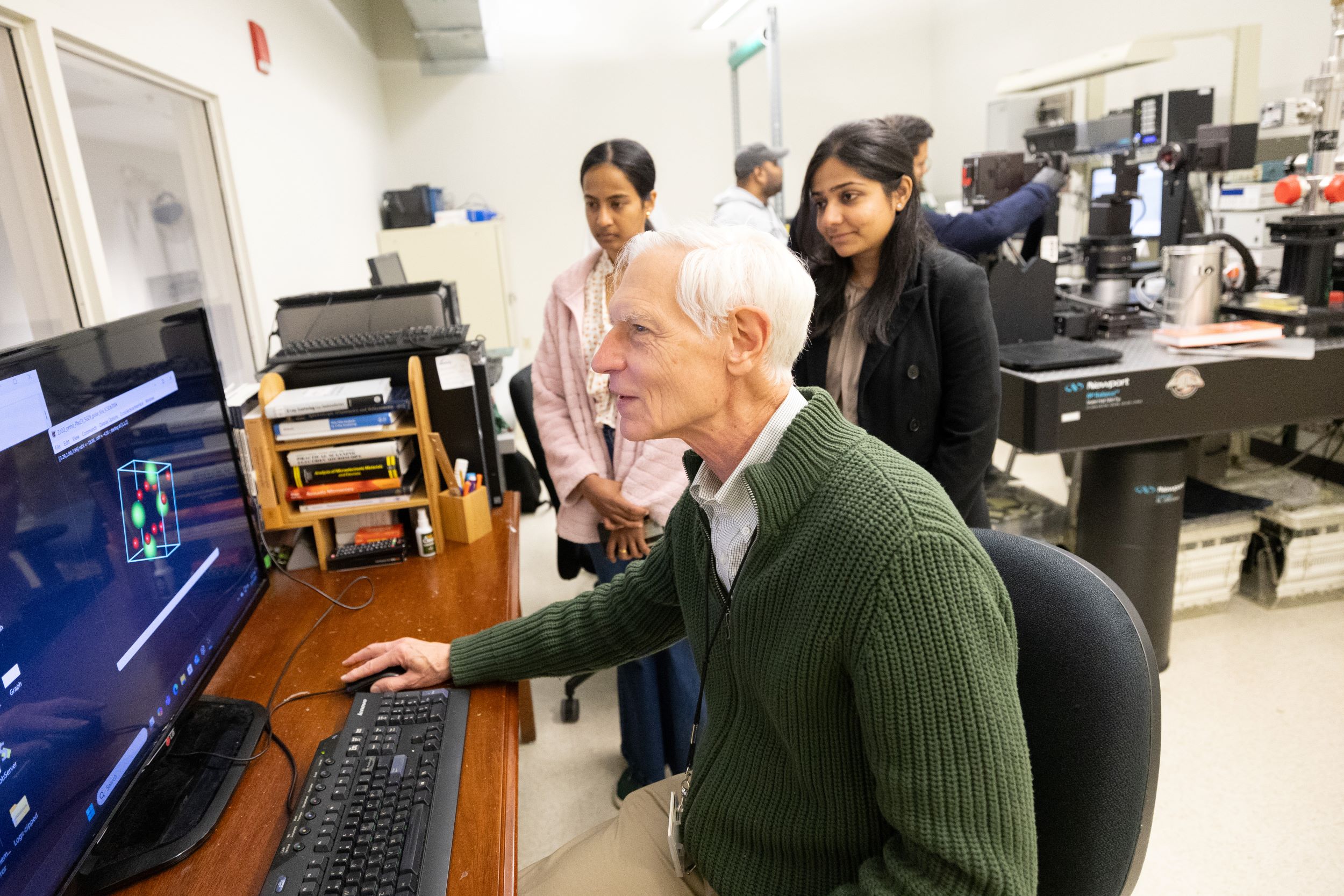
But with this ultrathin technology comes the glaring need to measure the different crystal phases of HZO, a process which is essentially automated due to the incredibly microscopic sizes involved. This is where College of Nanotechnology, Science, and Engineering (CNSE) Professor Emeritus and Empire Innovation Professor of Nanoscale Science Alain C. Diebold comes in.
Within Diebold’s lab, he and his students are keenly focused on materials characterization at the nanoscale level.
His recent paper, “Template Matching Approach for Automated Determination of Crystal Phase and Orientation of Grains in 4D-STEM Precession Electron Diffraction Data for Hafnium Zirconium Oxide Ferroelectric Thin Films,” takes aim at analyzing the different methods for mapping the thin film technology. It appears in the April issue of Microscopy and Microanalysis.
“Transistor technology has evolved over the years. In 2007, the industry started moving to dielectric layers, which have higher dielectric constant (High K) than silicon dioxide, which had been used up until that point,” explains Diebold. “The first layers were amorphous hafnium dioxide. This allowed further reduction in transistor dimensions. Subsequently, poly-crystalline layers of hafnium zirconium dioxide (HZO) were introduced.”
HZO is a particularly complementary metal-oxide semiconductor material that is already widely used in transistors or for memory storage. While this new technology is definitely a leap forward, it also requires new analytical tools to study the layers.
“HZO has several phases — or different crystal structures — with different dielectric constants. The thin HZO films are fabricated by Tokyo Electron (TEL) using atomic layer deposition processes,” said Diebold.
A typical thickness for these films is 10 nanometers, basically about the same as a few atoms stacked together.
“Recently, the goal has been to induce the orthorhombic, ferroelectric phase in these films,” said Diebold. “The challenge is that one of the orthorhombic phases is not ferroelectric but has a similar crystal structure to the ferroelectric phase.”
As Diebold explains it, the challenge is searching for the ferroelectric phase in the presence of other phases of HZO.
“Since X-ray measurements have large sampling areas, transmission electron microscopy and scanning transmission electron microscopy provide the necessary spatial resolution, and electron diffraction provides the ability to determine the phase and orientation of the grains of HZO in thin films,” said Diebold.
In the current study, Diebold and his collaborators used precession electron diffraction in a STEM to obtain high quality diffraction pattern maps of a cross-section of a 10-nanometer film stack.
“This map is referred to as 4DSTEM data — 2D from the map and 2D from the diffraction patterns at each pixel in the map,” said Diebold.
A single 4DSTEM map was used for this study. The goal was to compare automated algorithms for determining the phase and orientation represented by each diffraction pattern.
“The two algorithms found small differences in the amount of the ferroelectric phase in this film,” said Diebold. “This results in a question: Can machine learning improve the determination of phase and orientation?”
The next steps for Diebold’s lab include simulating precession electron diffraction data for training machine learning algorithms and testing various machine learning approaches.