JI UNG LEE RESEARCH GROUP

Ji Ung Lee Research Group

Ji Ung Lee

After 10 years in industry, Prof. Ji Ung Lee joined CNSE – SUNY Poly in 2007. Prof. Lee’s group focuses on fundamental studies of devices based on nanostructured materials.  They include carbon nanotubes, graphene, and other 2D materials.  The end applications include CMOS, post-CMOS, photovoltaic, photonic, and nanobio sensors.  We use SUNY Poly’s 300mm wafer line to fabricate devices and integrate these nanostructured materials onto unique device structures.

Electrical and Optical Properties of Carbon Nanotubes

Our group has pioneered the formation of p-n junctions using buried split gates in carbon nanotube, graphene, and 2D materials. The device properties include nearly ideal carbon nanotube p-n diodes and comprehensive probing of exciton transitions.

Graphene p-n Junctions

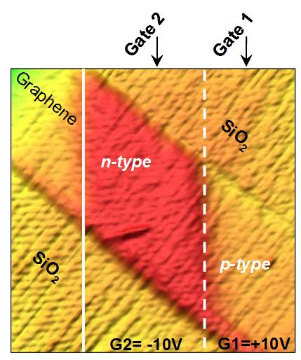
Our goal is to develop novel post-CMOS devices using graphene p-n junctions.  These are not rectifying junctions.  Instead, optics-like manipulation of carriers is possible based on the unique transport properties of these junctions.

Si CMOS Electronics

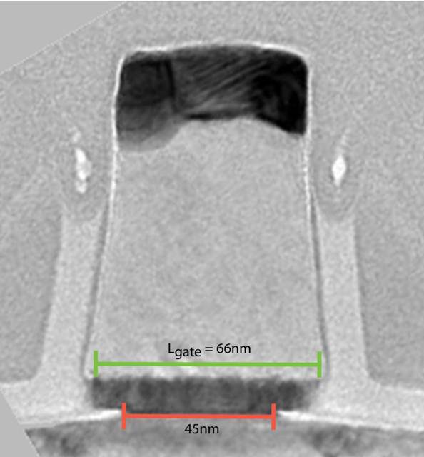
We characterized advanced Si CMOS devices, including nanowire gate all around FETs.  

Nanobio Applications

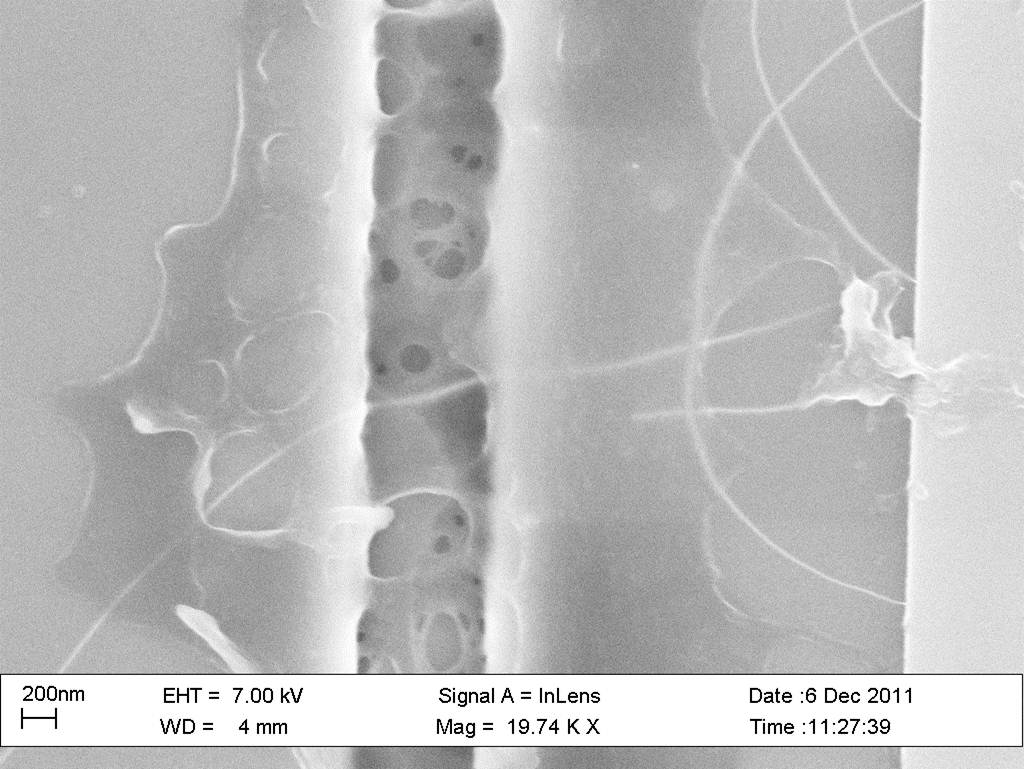
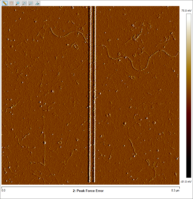
We are developing unique sensors to probe the internal metabolic reactions of individual cells and are examining the transport properties of DNA.

Teaching

Fall 2017:  NNSE 782: Topological Insulators:  Dirac Condensed Matter Systems (3 cr.)

Spring 2018:  NENG 406:  Fundamentals of Nanoelectronics (4 cr.)

Current Students

Graduate Students

  • Samuel LaGasse
  • Paul David
  • Prathamesh Dhakras
  • Luke Blanco
  • Sharadh Jois
  • Matt Zotta

Undergraduate Students:

  • Collin Sanborn
  • Samuel Skriloff

Recent Publications

1.     TID effects in reconfigurable MOSFETs using two-dimensional semiconductor WSe2, Prathamesh Dhakras, Pratik Agnihotri, Hassaram Bakhru, Harold L. Hughes, and Ji Ung Lee, IEEE Trans. on Nuclear Science, 09 November 2017.

2.     Three fundamental devices in one:  a reconfigurable multifunctional device in two-dimensional WSe2, P. Dhakras, P. Agnihotri, and J.U. Lee, Nanotechnology 28, 265203 (2017). (Featured in PhysOrg:  https://phys.org/news/2017-06-in-device-alternative-law.html, eeNews(Europe), https://www.eenewseurope.com/news/more-moore-2d-semiconductor-packs-3-functions-one-devicehttps://www.smart2zero.com/news/3-1-semiconductor-morphs-multiple-devices, electronicsweekly, https://www.electronicsweekly.com/news/business/sun-poly-makes-device-can-pin-diode-mosfet-bjt-2017-06/); https://www.elektormagazine.com/news/one-device-is-pin-diode-mosfet-or-bjt; http://www.europapress.es/ciencia/laboratorio/noticia-dispositivo-tres-alternativa-cumplir-ley-moore-20170614174633.html).

3.     Understanding magnetic focusing in graphene p-n junctions through quantum modeling, S.W. LaGasse and Ji Ung Lee, Phys. Rev. B 95, 155433 (2017).

4.     Theory of quantum transport in graphene devices with radiation induced Coulomb scatters, S. Lagasse, C. Cress, H. Hughes and J.U. Lee, IEEE Trans. On Nuclear Science, Vol. 2016.

5.     Zero-dark leakage current single-walled carbon nanotube diodes, Prathamesh Dhakras and Ji Ung Lee, Appl. Phys. Lett. 109, 203114 (2016).

6.     Theory of Landau level mixing in heavily graded graphene pn junctions, Samuel LaGasse and Ji Ung Lee, Phys. Rev. B,94, 165312 (2016).

7.     Large Bandgap Shrinkage from Doping and Dielectric Interface in Semiconducting Carbon Nanotubes, Everett Comfort and Ji Ung Lee,   Scientific Reports 6, Article number: 28520 (2016); June 24, 2016; doi:10.1038/srep28520

8.     Bipolar Junction  Transistors in Two-Dimensional WSe2 with Large Current and Photocurrent Gains, Pratik Agnihotri, Prathamesh Dhakras, and Ji Ung Lee* Article ASAP, Nano Lett  DOI: 10.1021/acs.nanolett.6b01444, June 23, 2016.  (Featured in Advances in Engr, https://advanceseng.com/nanotechnology-engineering/suny-poly-researchers-advance-bipolar-junction-transistors-two-dimensional-wse2-large-current-photocurrent-gains/)

9.     Reverse degradation of nickel graphene junction by hydrogen annealing Zhenjun Zhang, Fan Yang, Pratik Agnihotri, Ji Ung Lee, Jim R. Lloyd, AIP Advances 6, 025301 (2016)

10.  Edge-state transport in graphene p-n junctions in the quantum Hall regime, Nikolai N. Klimov, Son T. Le, J. Yan, Pratik Agnihotri, Everett Comfort, Ji Ung Lee, David B. Newell, Curt A. Richter, Phys. Rev. B 92, 241301 (R), 2015.

11.  Atomistic modeling of suspended carbon nanotube FET under proton irradiation, Samuel W. LaGasse,  Cory D. Cress, Harold  L. Hughes, Patrick J. McMarr and  Ji Ung Lee, IEEE Trans. On Nuclear Science, Vol. 62, pg 2881-2887, 2015.

12.  Characterization of magnetic Ni clusters on graphene scaffold after high vacuum annealing, Zhenjun Zhang, Akitomo Matsubayashi , Benjamin Grisafe , Ji Ung Lee, James R. Lloyd, Materials Chemistry and Physics 170, pg 175–179, 2015.

13.  Microstructure fabrication process induced modulations in CVD graphene, A. Matsubayashi, Z. Zhang, J.U. Lee and V. LaBella, AIP Advances 4, 127143 (2014).

14.  Disorder DOS in supported graphene, J. Appl. Phys. (2014), D. Sinha and J. U. Lee,

15.  Ideal Graphene/Silicon Schottky Junctions, Nano Lett 14, 4660 (2014), D. Sinha, J.U. Lee,

16.  Florence J. Nelson, Juan-Carlos Idrobo, John D. Fite,  Zoran L. Mišković, Stephen J. Pennycook,∥ Sokrates T. Pantelides,, Ji Ung Lee, and Alain C. Diebold, Electronic Excitations in Graphene in the 1–50 eV Range: The π and π + σ Peaks Are Not Plasmons, NanoLett, 2014

17.  Substrate dielectric effects in graphene field effect transistors, Zhaoying Hu, Dhiraj Sinha, Michael Liehr, and Ji Ung Lee, J. App. Phys. 115, 194507 (2014).

18.  Yong Q. An, J. E. Rowe, Daniel B. Dougherty, Ji Ung Lee, and Alain C. Diebold, Optical second-harmonic generation induced by electric current in graphene on the substrates of Si and SiC, Phys. Rev. B, 89, 115319 (2014).

19.  Journal of Radiation Effects Research and Engineering is a controlled DoD journal published by DTRA (2014) – collaborative publication with Harold Hughes (NRL).

20.  Intrinsic tolerance to total ionizing dose in gate-all-around MOSFETs, E. Comfort, M. Rodgers, W. Allen, S. Gausepohl, E.X. Zhang, M. Alles, H. Hughes, P. McMarr, and J.U.  Lee, IEEE Trans on Nuclear Science, VOL. 60, NO. 6, DECEMBER 2013, 4483-4487.

21.  Quantum Efficiency and Capture Cross Section of First and Second Excitonic Transitions of Single-Walled Carbon Nanotubes Measured through Photoconductivity, Argyrios Malapanis, Vasili Perebeinos,Dhiraj Prasad Sinha, Everett Comfort, and Ji Ung Lee, Nano Lett. 13,  3531–3538 (2013).

22.  Characterization of metal oxide layers grown on CVD graphene, A. Matsubayashi, J. Abel, D.P. Sinha, J.U.Lee and V.P. LaBella, J. Vac. Sci. Technol. A, 31, 021506 (2013).

23.  Enhanced optical second harmonic generation from the current-biased graphene/SiO2/Si structure, Yong Q. An, Florence Nelson, Ji Ung Lee and Alain Diebold, Nano Lett 13, 2104-2109, 2013.

24.  Single Cell In-Vivo Carbon Nanotube Device with Multimodal Sensing Potential Alexandra Scavelli, Abhishek Gottipati, Everett Comfort, Sabarinath Jayaseelan, Thomas Murray, Michael Rizzolo, Scott Tenenbaum and Ji Ung Lee, AIP Advances 3, 032122 (2013); (7 pages)

25.  Manifestation of chiral tunneling at a tilted graphene p-n junction, R.N. Sajjad, S. Sutar, J.U. Lee and A.W. Ghosh, Phys. Rev. B 86, 155412 (2012).

26.  Angle-dependent carrier transmission in graphene p-n junction, S. Sutar, E.S. Comfort, J. Liu, T. Taniguchi, K. Watanabe, and J.U. Lee, Nano Lett 12, 4460 (2012).

27.  Enhanced ultraviolet response using graphene electrodes in organic solar cells, Zhouying Zhao, John D. Fite, Pradeep Haldar, and Ji Ung Lee, Appl. Phys. Lett. 101, 063305 (2012).

28.  Single Exciton Quantum Logic Circuits, Ji Ung Lee,  IEEE J. of Quantum Electronics, Vol 48, No. 9, pp.1159-1164, September 2012.

29.  Parasitic capacitance removal of sub-100nm  p-MOSFETs using capacitance-voltage measurements, D.R. Steinke, J. Piccirillo, S. Gausepohl,  S. Vivekand, M. Rodgers, and Ji Ung Lee, Solid State Electronics, Vol. 68, pp 51-55,  Feb. 2012.

30.  Observation of the Urbach Tail in the effective density of states in carbon nanotubes, David A. Jones and Ji Ung Lee, Nano Lett. 11, 4176 (2011).

31.  Current-Induced Cleaning of Adsorbates in Single-Walled Carbon Nanotube Diodes, A. Malapanis, E. Comfort, and Ji Ung Lee, Appl. Phys. Lett. 98, 263108 (2011).

32.  Creation of individual defects at extremely high proton fluences in carbon nanotube    p-n diodes,   Everett S. Comfort, Matthew Fishman, Argyrios Malapanis, Harold Hughes, Patrick McMarr, Cory D. Cress, Hassaram Bakhru and Ji Ung Lee, IEEE Trans Nucl. Sci., vol 58, 2898-2903 (2011).

33.  Measuring Carbon Nanotube Band Gaps through Leakage Current and Excitonic Transitions of Nanotube Diodes, A. Malapanis, D. A. Jones, E. Comfort and J.U. Lee, NanoLett, 11, 1946 (2011).

34.  Spectroscopy of strongly localized excitons and band gap states in semiconducting single-walled carbon nanotubes, E.S. Comfort, D.A. Jones, A. Malapanis, Z.R. Robinson, M.T. Fishman, and J.U. Lee, Phys. Rev. B (Rapid Communications), 83, 081401(R), 2011 (Featured in Virtual Journal of Nanoscale Science and Technology, Vol. 23, Iss. 7, Feb. 21, 2011).

35.  Optical properties of large-area polycrystalline chemical vapor deposited graphene by spectroscopic ellipsometry, F. J. Nelson, V. K. Kamineni, T. Zhang, E. S. Comfort, J. U. Lee, and A. C. Diebold, Appl. Phys. Lett. 97, 253110 (2010).

36.  Reconfigurable multi-function logic based on graphene P-N junctions., Sansiri Tanachutiwat, Ji Ung Lee, Wei Wang, Chun Yung Sung, IEEE/ACM Design Automation Conference (DAC), pp. 883-888, June 2010.

37.  Bandgap renormalization in SWNTs:  Origin of the ideal diode behavior in carbon nanotube p-n structures, Ji Ung Lee, Phys. Rev. B, Vol 75, pp. 075409:1-5 (2007). (Featured in Virtual Journal of Nanoscale Science and Tech, Vol 15, Iss. 8)

38.  Direct probe of excitonic and continuum transitions in the Photocurrent Spectroscopy of Carbon Nanotube pn Diodes, Ji Ung Lee, Peter J. Codella, and Matthew Pietrzykowski, Appl. Phys. Lett., Vol 90, pp 053103:1-3 (2007). (Featured in Virtual Journal of Nanoscale Science and Tech, Vol 15, Iss. 6).

39.  Photovoltaic Effect in Ideal Carbon Nanotube Diodes, Ji Ung Lee,  Appl. Phys. Lett., Vol 87, pp 073101:1-3 (2005) (Cover article, August 15th, 2005). (Also featured in Virtual Journal of Nanoscale Science and Tech, local news).

40.  Evolution of charge emission for amorphous silicon FETs exposed to radiation, S. Zelakiewicz, A. Couture, S. Bogdanovich, J-U Lee and G. Possin, Nuclear Instruments and Methods in Physics Research A, Vol 546, pp 296-299 (2005).

41.  Carbon nanotube p-n junction diodes,  J. U. Lee, P. P. Gipp, and C. M. Heller Appl. Phys. Lett., Vol 85, pp 145-147 (2004) (Cover article, July 5th, 2004). (Featured in Physics Today (September, 2004), Popular Mechanics (October, 2004), Small Times, CNN, MSNBC, and other venues. Also featured in Virtual Journal of Nanoscale Science and Tech).

42.  Diffusion-limited transport in the off-state of amorphous Si thin-film transistors, J. U. Lee and G. E. Possin, Appl. Phys. Lett., Vol 82, pp 1302-1304 (2003).

43.  Interlayer phase correlation of the vortex system around the coupling transition in Bi2Sr2CaCu2Oy containing columnar defects Y. Tsuchiya, T. Hanaguri, H. Yasuda, A. Maeda, M. Sasase, K. Hojou, D. G. Steel, J. U. Lee, and D. J. Hofman , Phys. Rev. B, Vol 59, pp 11568-11574 (1999).

44.  Pinning effect on critical dynamics in Tl2Ba2CaCu2O8 films before and after introducing columnar defects, Jin-Tae Kim; Park, Y.K.; Park, J.-C.; Kang, W.N.; Chu, C.W.; Lim, H.R.; Kim, D.H.; Lee, J.U.; Gray, K.E.; Applied Superconductivity, IEEE Transactions on, Volume: 9 , Issue: 2 , pp 2296 – 2299, (June 1999).

45.  Observation of coherent modes of Josephson votices in Bi2Sr2CaCu2Ox, J.U. Lee, P. GuptasarmaD. HornbakerA. El-KortasD. Hinks, and K. E. Gray, Appl. Phys. Lett., Vol 71, pp 1412-1414 (1997).

46.  Effects of damping on the dynamics of Josephson votex in Bi2Sr2CaCu2Ox, Ji Ung Lee and James E. Nordman, Physica C, Vol 277, pp 7-12 (1997).

47.  Josephson vortex flow in superconducting single-crystal Bi2Sr2CaCu2Ox 
Ji Ung Lee, James E. Nordman, and Gert Hohenwarter, Appl. Phys. Lett., Vol 67, pp 1471-1473 (1995).

48.  RF coupling to single crystal BSCCO under c-axis bias
Hohenwarter, G.K.G.; Laundrie, A.W.; Lee, J.U.; Beyer, J.B.; Nordman, J.E.; Applied Superconductivity, IEEE Transactions on , Volume: 5 , Issue: 2 , pp 3195 – 3198 (June 1995).

49.  Low magnetic field sensitivity of c-axis transport in BSCCO (2212) single crystals, Ji Ung Lee; Hohenwarter, G.; Kelley, R.J.; Nordman, J.E.;Applied Superconductivity, IEEE Transactions on , Volume: 5 , Issue: 2 , pp 2543 – 2546 (June 1995).

50.  Magnetic field sensitivity of variable thickness microbridges in TBCCO, BSCCO, and YBCO, Davidson, B.A.; Redwing, R.D.; O'Callaghan, J.; Raissi, F.; Ji Ung Lee; Burke, J.P.; Hohenwarter, G.K.G.; Nordman, J.E.; Beyer, J.B.; Liou, S.H.; Eckstein, J.; Siegal, M.P.; Hou, S.Y.; Phillips, J.M.; Applied Superconductivity, IEEE Transactions on , Volume: 4 , Issue: 4 , pp 228 – 235 (December 1994).

51.  Effects of deposition conditions on stoichiometry of off-axis RF sputtered BiSrCaCuO thin films, Yang, Y.F.; Nordman, J.E.; Lee, J.U., Applied Superconductivity, IEEE Transactions on , Volume: 3 , Issue: 1 , pp 1543 – 1546 (March 1993).

52.  Effects of Target Presputtering on Stoichiometry of Sputtered Bi-Sr-Ca-Cu-O Thin Films, Y.F. Yang, J.U. Lee, J.E. Nordman, J. of Vac. Sci. and Tech. A, Vol 10, No. 5, pp 3288-3291 (September 1992).

Patents

1.     8,274,205 Systems and methods for limiting are effects in field emitter arrays, Wilson, Colin and Lee, Ji Ung, September 25, 2012.

2.     7,982,570 High performance low volume inductor and method of making same, Burdick, William, Lee, Ji Ung, and de Rooij, Michael, July 19, 2011.

3.     7,902,736 Gated nanorod field emitter structures and associated methods of fabrication, Hudspeth; Heather Diane, Lee; Ji Ung, Corderman; Reed Roeder, Zhang; Anping, Rohling; Renee Bushey, Denault; Lauraine, Balch; Joleyn Eileen, March 8, 2011.

4.     7,521,275 Free standing electrostatically doped carbon nanotube device and method for making same, Lee, Ji Ung; April 21, 2009.

5.     7,378,715  Free-standing electrostatically-doped carbon nanotube device, Lee, Ji Ung; May 27, 2008.

6.     7,329,552  Field effect transistor fabrication methods, field emission device fabrication methods, and field emission device operational methods,  Lee, Ji Ung; Lee, John; Moradi, Benham; February 12, 2008.

7.     7,326,328 Gated nanorod field emitter structures and associated methods of fabrication, Hudspeth, Heather Diane; Lee, Ji Ung; Corderman, Reed Roeder; Zhang, Anping; Rohling, Renee Bushey; Denault, Lauraine; Balch, Joleyn Eileen, February 5, 2008.

8.     7,239,076 Self-aligned gated rod field emission device and associated method of fabrication, Lee, Ji Ung; Corderman, Reed Roeder; Huber, William Hullinger, July 3, 2007.

9.     7,226,818 High performance field effect transistors comprising carbon nanotubes fabricated using solution based processing, Malenfant, Patrick Roland Lucien; Lee, Ji-Ung; Li, Yun; Cicha, Walter Vladimir; June 5, 2007.

10.  7,145,152   Storage capacitor design for a solid state imager, Lee, Ji Ung; Albaglie, D.; Possin, G.; Hennessy, W.A; Wei, C.Y.; December 5, 2006.

11.  6,943,495  Micro electro mechanical system controlled organic LED and pixel arrays and method of using and of manufacturing same, Ma, Kelvin; Lee, Ji Ung; Duggal, Anil, Sep. 13, 2005.

12.  6,890,780 Method for forming and electrostatically-doped carbon nanotube device, Lee, Ji Ung, May 10, 2005.

13.  6,784,434 Imaging array and method for manufacturing same Hennessy, William Andrew; Albagli, Douglas; Lee, Ji Ung; Wei, Ching-Yeu, August 31, 2004.

14.  6,777,685  Imaging array and methods for fabricating same, Lee, Ji Ung August 17, 2004.

15.  6,740,884 Imaging array and methods for fabricating same, Lee, Ji Ung; Albagli, Douglas ; Possin, George Edward; Wei, Ching-Yeu, May 25, 2004.

16.  6,710,539 Field emission devices having structure for reduced emitter tip to gate spacing,  Lee, Ji Ung, March 23, 2004.

17.  6,677,709 Micro electromechanical system controlled organic led and pixel arrays and method of using and of manufacturing same,  Ma, Kelvin; Lee, Ji-Ung; Duggal, Anil Raj,  January 13, 2004.

18.  6,559,506 Imaging array and methods for fabricating same, Lee, Ji Ung; Possin, George Edward, May 6, 2003.

19.  6,555,402 Self-aligned field extraction grid and method of forming, Wells, David H.; Lee, Ji Ung; Wilson, Aaron R., April 29, 2003.

20.  6,552,477 Field emission display backplates,  Lee, Ji Ung, April 22, 2003.

21.  6,504,170 Field effect transistors, field emission apparatuses, and a thin film transistor, Lee, Ji Ung; Lee, John; Moradi, Benham, January 7, 2003.

22.  6,464,550 Methods of forming field emission display backplates, Lee, Ji Ung, October 15, 2002.

23.  6,394,871 Method for reducing emitter tip to gate spacing in field emission devices,  Lee, Ji Ung, May 28, 2002.

24.  6,391,670 Method of forming a self-aligned field extraction grid,  Wells, David H.; Lee, Ji Ung; Wilson, Aaron R., May 21, 2002.

25.  6,344,378 Field effect transistors, field emission apparatuses, thin film transistors, and methods of forming field effect transistors, Lee, Ji Ung; Lee, John; Moradi, Benham, February 5, 2002.

Invited Talks

1.     Microelectronics Reliability and Qualifications Working Meeting, “TID Effects in Reconfigurable Nanostructured Devices”, Aerospace Corporation, LA, CA, Feb. 5-8, 2018.

2.     ET-CMOS 2017, “Three devices in one:  a reconfigurable multifunctional logic device in 2D TMDs”, Warsaw, Poland, May 28-30, 2017.

3.     Physics Colloquium, Bipolar Devices in Two Dimensional Material Systems for Novel Logic Applications, Rensselaer Polytechnic Institute, Troy, New York, January 25, 2017.

4.     2nd Annual The Society for Neuroscience Hudson-Berkshire Chapter, “The future of penetrating Neural Probes”, The Carey Institute for Global Good in Rensselaerville on Monday September 19, 2016. 

5.     “Overview of Photonics”, TEL Technology Center of America, Albany, NY, September 8, 2016.

6.     CMOS Emerging Technologies, Bipolar Devices in 2D Systems: Fabrication, Characterization and Applications, May 24-27, 2016. Montreal, Canada

7.     AVS 62 Meeting, 2D Bipolar Junction Devices for Novel Logic Applications:  Fabrication, Characterization, and Applications, October 18-23, 2015, San Jose, CA, USA.

8.     Workshop on Advanced Functional Material, AREX-UNESP, Araraquara, Sao Paolo, Brazil, August 3-6, 2015; Short course on “Quantum Transport: Principles to Applications”

9.     The 4th RJUS Symposium on Fundamental and Applied Problems in THz Devices and Technology, June 9-12, 2015, at Chernogolovka, Russia; “Graphene PN Junctions for THz Applications”.

10.  University at Buffalo-SUNY, Department of Electrical Engineering Graduate Seminar, Graphene PN Junction:  Interplay between Condensed Matter Physics, Quantum Electrodynamics, and post-CMOS Electronics, May 1, 2015, Buffalo, NY.

11.  GE Global Research, Langmuir Seminars:  Fundamentals of Graphene, April 13, 2015, Niskayuna, NY.

12.  SUNY Brain Network of Excellence Workshop 2014, CNSE Capabilities for Neural Probes; SUNY Buffalo, Clinical Translational Research Center, December 5-6, 2014, Buffalo, NY

13.  ENGE 2014, Logic Devices with Graphene p-n Junctions:  New Electron-Optics Devices , November 16-18, 2014, Jeju, South Korea.

14.  CMOS Emerging Technologies Research, Logic with GPNJs, July 6-8, 2014, MINATEC Grenoble, France.

15.  Armed Forces Communications Electronics Association (AFCEA), Command, Control, Communications, Cyber and Intelligence (C41) Technology Review Days and Exposition, Reconfigurable Logic with GPNJs, June 10-11, 2014.  Radisson Hotel Conference Center, Utica, NY

16.  Electrochemical Society (ECS) 225, Orlando, FL, Logic with graphene PNJunctions, May 11-15, 2014.

17.  Sematech Post CMOS Workshop Graphene PN Junctions:  New Electron-optics Devices – Washington DC, December 8, 2013.

18.  Albany Nanotech, Graphene PN Junctions, Albany, NY, August 2, 2013.

19.  IBM Alliance, Carbon Based P-N Junctions:  Fundamentals to Applications, July 30, 2013, Albany, NY

20.  CMOS Emerging Technologies Research 2013, Graphene pn Junction Devices; July 17-19, 2013, Whistler, British Columbia, Canada.

21.  2013 Device Research Conference, “Graphene PN Junctions for Electron-Optics Devices” June 23-26, 2013, U. of Notre Dame, Notre Dame, IN.

22.  2012 SPIE Optics and Photonics, Graphene pn junction devices: An Overview, August 12-16, 2012, San Diego, CA.

23.  221st Electrochemical Society Meeting, “Optical and Electrical Properties of Carbon Nanotube PN Diodes”, May 6-10, Seattle, WA, USA.

24.  221st Electrochemical Society Meeting, “Graphene PN Junctions”, May 6-10, Seattle, WA, USA

25.  International Symposium on Assessing the Economic Impact of Nanotechnology, “Measuring Economic Impact of Nanotechnology in Electronics – The New York State Investment Strategy”, March 27-28, 2012, AAAS, Washington, DC (In place of Michael Fancher).

26.  INDEX:  Graphene PN Junction Devices, Gov’t Microcircuit Applications and Critical Technology Conference (GOMAC) 12, March 19-22,Las Vagas, NV.

27.  Fabrication and Characterization of Graphene PN Junction Devices, American Vacuum Society 58th International Symposium and Exhibition, October 30-Nov. 4, 2011, Nashville, Tennessee (Presented by Surajit Sutar-post doc).

28.  7th International Nanotechnology Conference on Communication and Cooperation, Albany, NY, “INDEX Technical and Organizational Overview”, May 16-19, 2011.

29.  219th Electrochemical Society, “Probing Band Gap States in Carbon Nanotubes” Montreal, Canada, May 2-6, 2011.

30.  Carbon Based P-N Junction Devices, New York State Sectional Meeting of the American Physical Society, Albany, NY, April 8-9, 2011. (Substitute talk for Ann Swan).

31.  7th International Symposium on Advanced Gate Stack Technology, Sematech Symposium, “What do we really know about carbon nanotubes and why high-k dielectric matters”, Troy, NY, September 29-October 1, 2010.

32.  Center for Nanotubes and Nanostructured Composites, Sungkyunkwan University, “Optical Spectroscopy of Carbon Nanotube Diodes”, Suwon, Korea, August 25, 2010.

33.  IUMR-ICEM 2010 Conference, “Fabrication and Characterization of Graphene PN Junction Devices, Seoul, Korea, August 24, 2010.

34.  Sandia National Laboratory, Seminar on “Optical Spectroscopy of Carbon Nanotube PN Diodes”, Livermore, CA, July 13, 2010.

35.  Stanford University, Center for Integrated Systems, Seminar on “Graphene Veselago Device and Bilayer Graphene PN Junctions”  Stanford, CA, July 12, 2010.

36.  217th Electrochemical Society, “Probing Defects in Carbon Nanotubes Through Multi-Gated Structures” Carbon Nanotubes and Nanostructures:  Fundamental Properties, Vancouver, BC, Canada, April 27, 2010.

37.  217th Electrochemical Society, “Graphene Veselago Device:  Fabrication and Characterization of Graphene p-n  Junctions” Graphene Interfaces and Junctions, Vancouver, BC, Canada, April 26, 2010.

38.  IBM T.J. Watson Research Center, seminar on “INDEX Graphene Effort and Graphene P-N Junction Devices” Yorktown Heights, NY, January 5, 2010.

39.  Joint Workshop on Advanced Materials Research for Nanotechnology, joint between CNSE and National Institute for Materials Science (NIMS), Advanced Industrial Science and Technology (AIST) and the University of Tsukuba, all of Japan, “Graphene and Carbon Nanotube p-n Junction Devices” Albany, NY, December 10-11, 2009.

40.  Materials Science and Engineering Department, University of Wisconsin-Madison, “Carbon Nanotube and Graphene p-n Junction Devices”,  Madison, WI, October 8,9 , 2009

41.  3rd Workshop on Nanotube Optics and Nanospectroscopy, “Optical Spectroscopy of Carbon Nanotube Diodes”, Sendai, Japan, June 7-10, 2009.

42.  215th Electrochemical Society Meeting, Carbon Nanotubes and Nanostructures: Applications and Devices, “Fundamental Probe of Carbon Nanotubes Using Multi-gated Structures” San Francisco, CA, May 24-29, 2009.

43.  2009 International Conference on Frontiers of Characterization and Metrology for Nanoelectronics, “Overview of Carbon Based Nanoelectronics”, University at Albany, College of Nanoscale Science and Engineering, Albany, NY., May 11-14, 2009.

44.  NSF sponsored 6th US-Korea Forum on Nanotechnology:  Nanoelectronics and its Integration with Applications, “Optical Spectroscopy of Carbon Nanotube p-n Diodes” Las Vegas, NV, April 27-29, 2009.

45.  Modern Optics in Spectroscopy, Massachusetts Institute of Technology, “Optical Spectroscopy of Carbon Nanotube p-n Diodes”, Cambridge, MA., March 3, 2009.

46.  Seminar:  Dept. of Materials Science and Engineering, Gwangju Institute of Science and Technology, “Carbon Nanotube p-n Diodes” November 19-20, 2008, Gwangju, South Korea.

47.  55th American Vacuum Society Meeting, Manufacturing Science and Technology:  Beyond CMOS program: “Excitronics: Excitonic Circuits for post-CMOS Electronics”, October 19-24, 2008, Boston, MA.

48.  NSF sponsored French-American Young Engineering Scientists Symposium (YESS 2008), “Excitronics:  Excitonic Circuits for post-CMOS Electronics”, July 7-9, 2008, Washington DC

49.  213th Electrochemical Society Meeting, Carbon Nanotubes and Nanostructures: Applications and Devices, “Carbon Nanotube p-n Diodes” Phoenix, Az., May 20, 2008.

50.  213th Electrochemical Society Meeting, Carbon Nanotubes and Nanostructures:  Fundamental Properties and Processes, “Probing Excitonic Properties of Individual Nanotube p-n  Diodes”, Phoenix, Az., May 19, 2008.

51.  Physics Colloquium, Lehigh University, “Carbon Nanotube p-n Junction Diodes”, April 3, 2008, Bethlehem, PA.

52.  FENA/ONAMI:  Workshop on Nanoelectronics for High Performance Computing and Information Processing, “Carbon Nanotube Excitonics”, UCLA, November 19-20, 2007.

53.  2007 IEEE Lasers and Electro Optical Society (LEOS – Annual Meeting), “Carbon Nanotube P-N Junction Diodes”,  Orlando, FL, October 21-25, 2007.

54.  6th Annual Center for Optical Technologies, “Carbon Nanotube p-n Junction Diodes”, Lehigh University, Bethlehem, PA, October 8-9, 2007.

55.  Corning Inc., “Nanoelectronics at CNSE”, Corning, NY, August 3, 2007.

56.  IEEE Lasers and Electro Optical Society (LEOS – Summer Topical Meetings on Biophotonics), “Excitons in Biological and Non-Biological Nano-Structured Systems:  Progress Towards Bio-inspired Photodetectors”,  Portland, Oregon, July 23-25, 2007.

57.  2nd Workshop on Nanotube Optics and Nanospectroscopy, “Probing Excitonic and Continuum Transitions in SWNT p-n Diodes”,  Ottawa, Canada, June 4-7, 2007.

58.  Brookhaven National Laboratory, Center for Functional Nanomaterials, “Carbon Nanotube p-n Junction Diodes”, Upton, NY, April 30, 2007.

59.  Nanoscale Science and Engineering Center, Columbia University,  “Examination of Interplay between Transport and Optical Properties in Single-Walled Carbon Nanotubes”, New York, N.Y., April 11, 2007.

60.  American Physical Society – March Meeting, “Interplay Between Transport and Optical Properties in Carbon Nanotube p-n Diodes”, Denver, CO., March 5-9, 2007.

61.  Department of Chemistry, University of Montreal, “Optical Response of Single Walled Carbon Nanotubes”, Montreal, Canada, Feb. 26, 2007.

62.  Printed Electronics USA 2006, “Reconfigurable Carbon Nanotube Switch”, Phoenix, Az., December 5-6, 2006.

63.  American Chemical Society National Meeting, Presidential Event, “Carbon Nanotube p-n Junction Diodes”, San Francisco, CA., September 10-13, 2006.

64.  Emerging Information Technology Conference, “Carbon Nanotube p-n Junction Diodes”, University of Texas, Dallas, TX, August 9-11, 2006.

65.  2006 IEEE Electron Device Conference: Lester Eastman Conference on High Performance Devices, “Carbon Nanotube P-N Junction Diodes”, Cornell University, Ithaca, NY, August 2-4, 2006.

66.  NSF/ONR Review of North American R&D on Carbon Nanotube Manufacturing and Applications, “Carbon Nanotube p-n Junction Diodes” NSF, Arlington, VA, June 2, 2006

67.  GE Power Electronics Symposium, “Reconfigurable Carbon Nanotube Switch”, GE Global Research, Sep 1-2, 2005.

68.  Dupont Central Research and Development, “Electronics with Carbon Nanotubes”, Wilmington, DE., May 18, 2005.

69.  Center for Nanoscale Systems Symposium:  Nanoelectronics – From Discovery to Systems, Cornell University, “Electronics with Carbon Nanotubes:  p-n Junction Diodes”, Ithaca, NY, April 6, 2005.

70.  Center for Nanoscience and Nanobiotechnology, Boston University, “Carbon Nanotube p-n Junction Diodes”, Boston, MA., March 10, 2005.

71.  Dept. of Electrical Engineering, Union College, “Carbon Nanotube p-n Diodes” Schenectady, NY, November 2004.

72.  12th NSF Workshop on Materials Science and Nanotechnology, “Electronics with Carbon Nanotubes: Critical Role of Contacts”, Broomfield, CO., Oct. 28-31, 2004.

73.  International Electronics Packaging Symposium, National Trends in Small Scale Systems and Microelectronics Packaging, Binghamton University and GE Global Research, Oct. 19-20, 2004, GE Global Research, Niskayuna, NY.

74.  Institute of Electrical and Electronics Engineering-Nano 2004, “Carbon Nanotube p-n Junction Diodes”, Munich, Germany, August 16-19, 2004 (Plenary Talk).

75.  Air Force Office of Scientific Research sponsored conference on Flux, Quantum and Mesoscopic Effects in Superconducting Materials and Devices, “Josephson Vortex Flow in  BSCCO”, Santa Fe, New Mexico, August 4-8, 1997.

76.  1997 International Symposium on Intrinsic Josephson Effect and THz Plasma Oscillations in High Tc Superconductors, “Josephson vortex dynamics in superconducting BSCCO” Sendai, Japan, Feb. 23-24

Images


Si MOSFET fabricated at CNSE


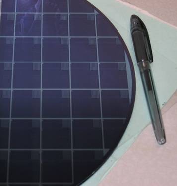
One of our wafers with buried gates


Surface potential map of our graphene p-n junction


A Carbon Nanotube threading a single cancer cell


Electrical contacts to DNA


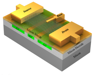
Bipolar Junction Transistor in 2D Transition Metal Dichalcogenide Semiconductors