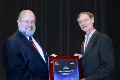
Alain Diebold
Empire Innovation Professor of Nanoscale Science
Executive Director Center of Nanoscale Metrology
Executive Director New York Center of National Competitiveness in Nanoscale Characterization (NC)3
[email protected]
Professor Diebold received his PhD from the Department of Chemistry at Purdue University in 1979 under the guidance of Professor Steve Ademan. His thesis was titled: A Generalized Langevin Equation Approach to Gas – Solid Surface Scattering. His post-doctoral work was with Professor Nick Winograd at Pennsylvania State University in the area of angle resolved secondary ion mass spectrometry studies of single crystal surface phenomena. Alain recently became a professor at the College of Nanoscale Science and Engineering at the University at Albany. His research will focus on the impact of nanoscale dimensions on the physical properties of materials; he also continues to work in the area of nanoelectronics metrology.
He is an AVS Fellow, SPIE Fellow, and was a SEMATECH Senior Fellow, He chaired the International Metrology Technical Working Group for the ITRS. When the IC industry roadmap started, he founded and co-chaired the U.S. Metrology Technical Working Group. For many years, he was chair of the Manufacturing Science and Technology Group of the American Vacuum Society. As SEMATECH Senior Fellow, the main focus of his activities involved international metrology coordination between industry, national laboratories and academia. He has edited the Handbook of Silicon Semiconductor Metrology, published in June 2001. He was a Panel Member for the Metrology section of Future Fab International. He also worked at Allied Signal in the areas of molecular beam epitaxy of III-V compounds and materials characterization of a broad range of semiconductor and amorphous metal products.
Pod casts on Metrology featuring Dr. Diebold can be found at:
Romaine Sanju
Romaine Sanju is a PhD student at University at Albany, State University of New York in the class of 2024. She has graduated from a prestigious State University in Sri Lanka with a B.Sc degree with honors in Physics. For her undergraduate research project, she has been able to develop Lightweight Multifunctional Carbon Nanotubes Incorporated Cellular Natural Rubber Composites (CNRCs) by incorporating Carbon Nanotubes (CNT) as a substitute for the conventional filler Carbon Black (CB).
Sanju also completed her Master of Science education in Taiwan at National Sun-Yat Sen University. There, she researched van der-Waals layered bulk V2IV2VI6 (V= Sb or Bi; IV = Si, or Ge; VI = S, Se, or Te) compounds for topological and thermoelectric applications. She also has experience in using ab initio codes, many-body physics as well as electronic structure theory, and different methods such as density functional theory (DFT) as well as classical and ab initio molecular dynamics simulations. Currently she is using computational methods such as DFT and NEGF to understand unconventional resistivity scaling in 2D material for potential application to next generation microprocessors.
Alumni Members
Ezra Mel Pasikatan
Metrology Engineer at ASML
Ezra Pasikatan is a PhD candidate at SUNY Polytechnic Institute. The topic of his dissertation is Advanced Characterization and Metrology of 3D Memory film Stacks and Structures using Mueller Matrix Ellipsometry based Scatterometry. Ezra obtained a masters in nanoscale engineering at SUNY Poly in 2022 and has a bachelor's in chemical engineering from Oregon State University. Before going to graduate school, he spent eight years in the semiconductor industry as an engineer at ASML and Wafertech (TSMC Fab 11). As an applications engineer at ASML, he helped introduce a type of diffraction-based overlay metrology capital equipment into a customer's technology development Fab in Hillsboro, Oregon. He also has managed mature fab toolsets ranging from defect review, thin film, overlay and SEMs as a metrology equipment engineer at Wafertech. His goal is to contribute as to projects at the cutting edge of semiconductor technology.
Madhulika Korde
Metrology Engineer at Nova
[email protected]
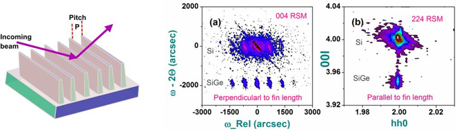
Ms. Madhulika Korde is a PhD graduate student at SUNY Polytechnic Institute in Albany, NY. Her current research focuses on the characterization of Si/SiGe FinFETs and contact holes for Gate-All-Around Transistors for the development of advanced technology nodes. The most critical metrology techniques used for this project are Scatterometry, Reciprocal Space X-Ray Diffraction and Critical-Dimension Small Angle X-Ray Scattering. In addition, she has formal training in diverse metrology techniques, semiconductor devices, process control and has studied organic emulsion stability. She is eager to explore the numerous opportunities available in the fields of nanoelectronics, nanoarchitecture and metrology. Madhulika completed her Bachelor’s in Chemical Engineering at the Institute of Chemical Technology, Mumbai, India.
Her previous work includes organic polymer based-photovoltaic cells, emulsification and de-emulsification technology and the study of magneto-caloric materials. Her novel work on the de-emulsification of an organic industrial mixture provided a practically feasible solution and has been integrated into the compound synthesis process by VAL Organics India Ltd. Her strong interest in materials and their integration into functional devices drove her towards pursuing Nanoscale Engineering at The College of Nanoscale Science and Engineering at SUNY Polytechnic Institute. Looking ahead, she would like to contribute towards the development of novel 3D structures using optimized functional materials for the semiconductor industry.
Amir Kordijazi
Interdisciplinary Materials Scientist
[email protected]
Amir Kordijazi is an interdisciplinary materials scientist with research interest in applying data science and materials informatics techniques in design, synthesis, characterization, and optimization of advanced nanoscale materials. He received his PhD with a major in Industrial & Manufacturing Engineering and a minor in Materials Science & Engineering from the University of Wisconsin, Milwaukee, in 2021.
His doctoral research focused on applying data-driven techniques to design adsorbent materials for water treatment application. He subsequently joined the College of Nanoscale Science and Engineering at SUNY Polytechnic Institute, NY, as a postdoctoral associate. He is currently working at the Center of Metrology in close collaboration with a group of scientists from Tokyo Electron US to apply artificial intelligence and machine learning for design, characterizations, and optimization of new generations of nanoscale semiconductor materials."
Colin Wadsworth
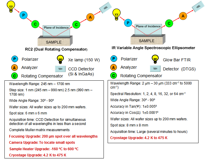
Colin Wadsworth graduated SUNY Polytechnic Institute College of Nanoscale Science and Engineering with a bachelors in Nanoscale Science and a minor in physics in 2022 with a focus in characterization and metrology of different nanoscale structures. Research areas are using different measurement techniques to analyze nanoscale structure such as Mueller Matrix Ellipsometry based scatterometry and XRD. He also trains graduate and undergraduate students in using the RC2 ellipsometer and the CompleteEase software to measure and model different structures.
He interned at Global Foundries working in the Optical Hybrid Metrology group, where he helped optimize different optical models to improve the accuracy of critical dimension measurements. Currently a graduate student at the University of Minnesota pursuing a doctorate in material science. In the future, he hopes to contribute to the material science field through understanding and discovering new materials and their behaviors.
Vineetha Mukundan
Research Scientist
[email protected]
Vineetha Mukundan joined the group as a postdoctoral associate in October 2017. She obtained her PhD in Physics from Purdue University, Indiana, USA in 2014 (Dissertation: Structural characterization of multimetallic nanoparticles). Before coming to CNSE, she has worked on materials characterization of fuel cell catalytic nanoparticles, molecular electronics and fluid mechanics of clay particles.
She has sustained interests in areas of condensed matter physics, statistitical mechanics and non-linear dynamics. Her main role at CNSE is to provide materials characterization and metrology by different techniques (including synchrotron based) of high k-dieletric thin films developed by TEL Technology Center, America for the continued scaling of CMOS devices. While not at work, Vineetha pursues amateur photography, traveling, hiking in the woods and Indian classical carnatic music.
YongQiang An
YongQiang An received his PhD in Physics from the University of Colorado at Boulder in 2003, in the area of optical second-harmonic generation at Si surfaces. Thereafter, he worked as a postdoc at the University of California at Berkeley (2003-2004), the University of Texas at Austin (2004-2008), and Los Alamos National Laboratory (2008-2011), on a variety of projects in the areas of nonlinear optics and ultrafast spectroscopy. He developed a new technique for measuring the phase of second-order susceptibility tensors and his work on UO2 opened a new field of research-ultrafast dynamics of 5f electrons. Y. Q. An has continued to pursue his research goals in femtosecond spectroscopy of electronic materials, joining the group in 2012.
Sonal Dey
Metrology Engineer (GLOBALFOUNDRIES)
Sonal Dey joined the group as a postdoctoral associate in December, 2014. He obtained his PhD in Physics from Kent State University, Ohio, USA in 2013 (dissertation title: Elasticity of Main Chain Liquid Crystal Elastomers and its Relationship to Liquid Crystal Microstructure). Before coming to CNSE, he worked as a postdoctoral research associate with Prof. Robert Mayanovic at Missouri State University, investigating the physicochemical properties of various functional nanoscale and mesoporous materials and structure-property relationship and theoretical modelling in glasses, melts and amorphous materials. His primary responsibility is to provide the metrology R&D efforts (both at synchrotron facilities and at CNSE) necessary for characterizing the next generation high-k dielectric films and metal gate materials, developed in a collaborative research program between TEL Technology Center, America and Professor Diebold’s Research group. Apart from research, Sonal enjoys playing chess and likes to travel.
Avery Green
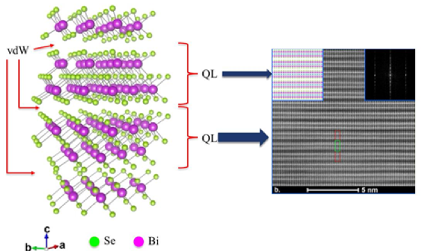
Avery Green received a BS in Physics with a minor in Mathematics from the University of California at San Diego. While working on his BS degree, he worked in an isotopic chemistry lab, designing and building a thin film deposition system in order to model isotopic reactions on the surfaces of meteors. He joined the group in 2013, and is currently working on Topological Insulator-related metrology.
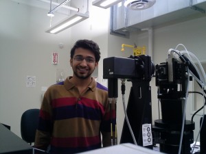
Sam O’Mullane
Applications Scientist (Nanometrics)
PhD Nanoscale Science, 2015
Sam received his MSc. in Quantum Field & Fundamental Force Theory from Imperial College London in 2013 and his BS in Physics from Boston College in 2012. He defended his thesis on plasmonic enhancements in ellipsometric measurements of metal lines in November 2015. He currently works on scatterometry for Nanometrics.
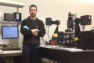
Dhairya Dixit
Metrology Engineer (GLOBALFOUNDRIES)
PhD Nanoscale Engineering, 2015
Dhairya received a BS in Metallurgy and Materials science Engg (2008 – 2012) from Faculty of Technology and Engineering (Maharaja Sayajirao University, Baroda). His project was Characterization and property evaluation of CuInSe2 thin film prepared from nanocrystalline powder. He completed and defended his thesis on semiconductor-related CD scatterometry in August 2015, and is currently working on scatterometry for IBM.
Relja Vasic
Postdoctoral Research Associate (2011-2014)
PhD Physics, Florida State University (2007)
Relja received his PhD in Physics from the Florida State University at the National High Magnetic Field Laboratory in 2007. Later, he worked at National Research Council as a postdoctoral fellowship at North Carolina State University studying multiferroic materials. worked on the characterization of high k gate dielectrics.
Manasa Medikonda
Metrology Engineer (GLOBALFOUNDRIES)
PhD Nanoscale Engineering, 2014
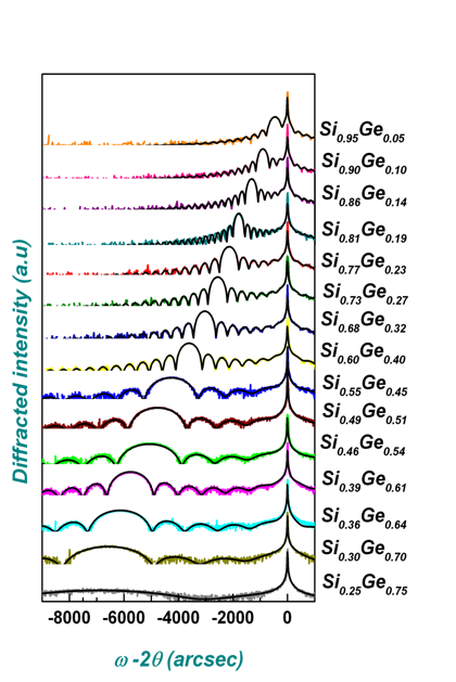
Manasa Medikoda received her Masters of Science Degree in Electrical Engineering, Polytechnic Institute of New York University, NY in 2011 and Bachelor’s degree in Electronics & Communications Engineering from MVIT college, Bangalore, India in 2008. She completed and defended her thesis on High resolution X-ray diffraction and optical characterization of fully strained pseudomorphic SiGe and GeSn alloy layers in July 2014, and is currently working in engineering for Global Foundries.
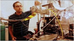
Gangadhara Raja Muthinti
Metrology Engineer (IBM)
PhD Nanoscale Engineering, 2013
Gangadhara Raja Muthinti received his B.E in Chemical Engineering from Andhra University College of Engineering, India in April 2007. Later, he joined the Department of Chemical & Bio-Molecular Engineering at Clarkson University, New York in Fall 2007 to perform research on Process Intensified (PI) Modules for process industries. His research was to understand and predict the mass transfer characteristics of a Rotating Tube Reactor (RTR), one of the state of the art intensified modules present in the field of Process Intensification. He graduated in December 2009 and received his Master’s Degree in Chemical Engineering. Later, he worked as an intern for a start up company R3 Fusion Inc., Troy, NY and was a lead member in designing and installing a patent pending process module for several industrial clients. He joined the group in Fall 2010 and graduated with his PhD in Nano Engineering at the University at Albany-SUNY in 2013, in The College of Nanoscale Science and Engineering.
Florence Nelson
Metrology Engineer (IBM)
PhD Nanoscale Engineering (2012)
Florence Nelson received a BS in Electrical Engineering, Minor in Computer Science, from State University of New York at New Paltz in December 2007. From 2004-2008 she worked at IBM Poughkeepsie in the Server Technology Group as a Product Safety and EMC intern.
LayWai Kong
DETD/Senior Process Engineer (Intel)
PhD Nanoscale Engineering (2011)
LayWai received a BS in Applied Physics and a Minor in Music from University Sains Malaysia in May 2005. After her graduation she worked as a Failure Analysis Engineer for National Semiconductor, Malaysia. With her industrial experience she joined University of Massachusetts Dartmouth for her Masters in Physics and graduated in 2008. She worked on Microfluidics-Nitrate Sensor ( Master’s Thesis). She later joined Dr. Diebold’s group and worked on IR and Acoustic microscopy of 3-D interconnects.
Vimal Kamineni
Principal Research Engineer (GLOBALFOUNDRIES)
PhD Nanoscale Science (2011)
Vimal Kamineni received a dual degree in BE in Electronics & Instrumentation and a MS in Physics from Birla Institute of Technology & Science in Pilani in December 2004. He joined Louisiana Tech University in fall 2005 and worked on advanced characterization techniques (EXAFS & XANES) at Center for Advanced Microstructures & Devices, Baton Rouge. His research at Louisiana Tech University was on hydrogen storage materials (supported by the National Science Foundation, Division of Materials Research), and he graduated with a dual degree in MS in Molecular Science & Nanotechnology and a MS in Microsystems Engineering. He joined the group in fall 2007 and is pursuing his PhD in Nanoscale Science at the University at Albany-SUNY, in The College of Nanoscale Science and Engineering. He worked on the development of robust optical models for thin metal films using Variable Angle Spectroscopic Ellipsometry (VASE). He also characterized the pore size, shape, distribution and interconnectivity in porous low-k dielectrics using X-ray Reflectivity (XRR), Transmission Electron Microscopy (TEM) and the IBM-X20 beam lines at the National Synchrotron Light Source at Brookhaven National Laboratory in New York.
Tianhao Zhang
Senior Engineer (KLA-Tencor)
Postdoctoral Research Associate (2011)
PhD Physics, University of Colorado (2008)
Tianhao Zhang received the PhD degree in Physics in May, 2008 from JILA, a joint institute of NIST and University of Colorado at Boulder. Under the direction of Dr. Steven T. Cundiff, he developed optical two-dimensional Fourier-transform spectroscopy as a novel technique for the studies of exciton dynamics, many-body interactions, and disorders in semiconductor nanostructures. He started postdoctoral research in the group in Nov. 2008, and worked on the characterization of nanoscale materials and structures with linear and nonlinear optical methods including second harmonic generation and photoreflectance. He received BS and MS degrees from University of Science and Technology of China before coming to USA.
Eric Bersch
Metrology Engineer (GLOBALFOUNDRIES)
Postdoctoral Research Associate (2011)
PhD Physics, Rutgers University (2008)
Eric Bersch graduated from Rutgers University with a PhD in Physics in July, 2008. At Rutgers, he worked under the direction of Dr. Robert Bartynski using photoemission and inverse photoemission spectroscopies to measure the energy level alignment of two types of material systems: metal/oxide/semiconductor stacks with high-k oxides and organic dye/oxides. A third project he worked on was the measurement of the electronic structure of the stoichiometric and reduced SnO2(101) surface. Previous to his work at Rutgers, he taught physics and coached basketball and soccer at Pompton Lakes High School for 5 years.
Joshua LaRose
MS Nanoscale Engineering (2011)
Applications Engineer (Tokyo Electron Ltd)
Joshua LaRose received a BS in Physics with a minor in Mathematics from the State University of New York at Albany in May 2009. While working on his BS degree, he worked on ion beam materials analysis, as well as rare Earth doped Silicon crystals for spintronic applications. He joined the group in 2009, and worked on the characterization of High-k gate dielectrics
Ming Di
PhD Nanoscale Science (2010)
Applications Manager (KLA-Tencor)
Ming Di received a BS in Physics from Fudan University, Shanghai, China in May 2002. He has received his PhD at the University at Albany-SUNY, in the College of Nanoscale Science and Engineering and his thesis title is”INVESTIGATION OF THE THRESHOLD VOLTAGE SHIFT EFFECT OF La2O3 ON TiN/HfO2/La2O3/SiO2/Si STACKS”.