Biological
Dr. Cady operates a 1,500 sq ft laboratory with 30 oC & 37 oC incubators (both CO2 and non-CO2 equipped), -80 oC and -20 oC freezers, +4 oC refrigerators, chemical solvents and acid fume hoods, a Class II/A2 biological safety cabinet, Nikon 80i epifluorescence microscope with a cooled QICam CCD camera, Leica SP5 confocal laser scanning microscope (CLSM), Nikon dissecting/stereomicroscope, two Fisherbrand inverted phase contrast microscopes, Veeco Bioscope Catalyst atomic force microscope (AFM), Tecan M200 microplate fluorometer/luminometer with UV/VIS spectrophotometer capability, BioRad real-time PCR thermocycler, BioRad Protean II gel electrophoresis equipment, BioRad Versa Doc fluorescence/luminescence/bright field documentation system, centrifuges, autoclave, Nanodrop ND1000 UV-vis spectrophotometer and ND3300 fluorometer, Malvern Nano-ZS dynamic light scattering (DLS)/zeta potential instrument, Akta FPLC system, multiple KD scientific and Harvard Apparatus syringe pumps, and all other general laboratory equipment needed for cell growth and maintenance, protein chemistry and biochemical analysis in the proposed research.
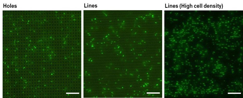
The labs are equipped with a humidity controlled Scienion sciFLEXARRAYER S3 and an ArrayIt Spot Bot platform for molecular printing (antibodies, proteins, etc.) installed next to cell incubators and fluorescent microscopes. In addition, to the described biological laboratories, the PIs can utilize existing facilities at CNSE including all available metrology, surface analytical tools and electron/visual microscopy.
Further, the lab has a Ciencia, Inc. grating-coupled surface plasmon resonance (GC-FP) detection instrument on-site, which can be used for the GC-FP experiments proposed, as well as an Elveflow OB1 automated microfluidic control system.
Electrical Testing & Evaluation
Prof. Cady maintains an electronics testing laboratory with ~500 sq. ft. of space which can be used for evaluation and analysis of electronic devices. The electronics testing laboratory contains a faraday cage enclosed Cascade M150 8” manual probe station, and a Wenesco 8” HP99D thermal stage. Electrical source and measure is carried out by an Agilent B1500A semiconductor parameter analyzer with DC and pulsing measurement capability, and associated Lenovo E30 workstation running Agilent EasyExpert software for data collection and analysis.
Additional electrical test equipment is available in a 900 sq. ft. lab space containing four major probers. These include two Cascade Microchamber test stations equipped with an Agilent B1500A semiconductor device analyzer, Keithley 708B switching matrix, Agilent E4908A precision LCR meter, Agilent 81110A pulse/pattern generator, Keithley 4200-SC5 semiconductor characterization system, Keysight N7744A optical power meter, Keithley 2613 system source meter and Keysight 8163B lightwave multiplier.
There are two Suss Microtech semi-automated probe stations. These are equipped with Agilent B1500A semiconductor device analyzer, Agilent N5227A PNA network analyzer (10MHz-67GHz), WavePro 740Zi 4GHz oscilloscope, Anritsu 37369D vector network analyzer, HP 4145B semiconductor parameter analyzer, Agilent 3560A dynamic signal analyzer and ProPlus 9812B noise analyzer controller.
There is also a Suss Microtech cryogenic test station capable of operating at LN2 temperatures in vacuum to 1E-5torr.
Nano/Micro Fabrication Facilities & Capabilities
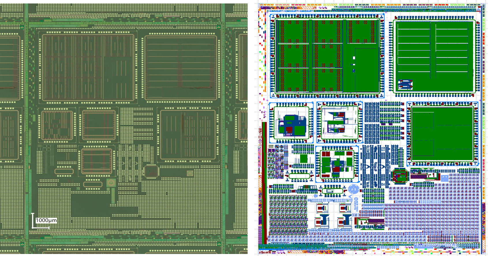
Dr. Cady has full access to the Albany NanoTech nanofabrication complex for all nano/microfabrication tasks. The fabrication facilities located at its Albany NanoTech Complex house more than 120 wafer processing and inline metrology tools. The tool sets installed in these world-class facilities are dedicated to supporting the industry's wafer processing needs for the next several device generations ranging from 65nm to 2nm, and allowing exploratory work in support of full-scaled nanotechnology.
Albany NanoTech's next-generation facilities are currently operational with a fully enabled 65nm low power CMOS and RF CMOS offering. These fabrication facilities also produce integrated silicon photonics multi project wafers (MPW) and private/custom production runs. Early user hardware, custom R&D and on-demand derivative development support is provided at Albany NanoTech with access to unique state-of-the-art industry standard semiconductor fabrication facilities, which serves as a technology test-bed leading to the development, demonstration, integration and qualification of advanced fabrication technologies for the semiconductor industry.
The Albany NanoTech facilities house 300mm advanced lithography platforms to support 193nm immersion lithography development and EUV lithography development. Also installed are advanced wafer platforms for planarization, copper plating, etch development, ion implantation, thin film development and wet cleaning technology. In total, the nanofabrication complex houses the latest nanofabrication technology available, and house all the technology and equipment needed for the proposed project including resist spinners, UV immersion steppers, nanoimprint lithography, EUV lithography, E-beam lithography, PVD, CVD, PECVD and ALD deposition tools, chemical mechanical planarization (CMP) reactive ion etching, acid/base and solvent fume hoods.
Albany NanoTech / UAlbany nano/micro fabrication facilities are broken down into the following sections, with these general capabilities: NanoFab 300 North is a 228,000 square foot, $175 million facility including 35,000 square feet of cleanroom space with Class 1 capable 300mm wafer production. NanoFab 300 South is a 150,000 square foot, $50 million facility including 32,000 square feet of cleanroom space.
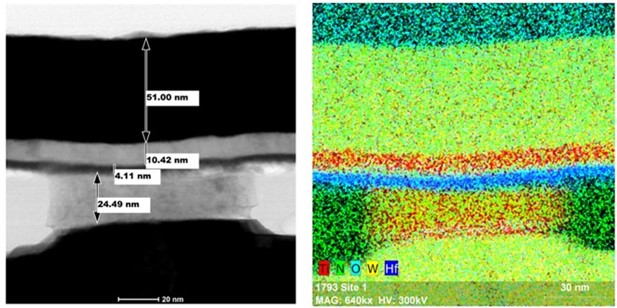
The facility also includes classrooms and offices for UAlbany faculty. NanoFab 200 (also known as CESTM) is a 70,000 square foot facility that includes additional 4,000 square feet of cleanroom space, plus metrology labs. Equipment in this facility includes resist spinners, contact aligners, RIE etchers, evaporative and atomic layer deposition (ALD) thin film deposition tools, a plasma-based ashers, thermal annealing chambers and furnaces. Metrology equipment includes focused ion beam (FIB) sample preparation, X-ray diffraction, TEM, SEM, XPS, SIMS, and Auger spectroscopy.
NanoFab Central, a 100,000-square-foot building that houses 15,000 square feet of 300mm wafer, class 1 capable cleanroom space, and NanoFab East, a separate 250,000-square-foot office, laboratory and classroom building.
The newest building on-site to include fabrication facilities is NanoFabX, which was completed in 2013, and is a 500,000-square-foot facility with 50,000 square feet of 300mm wafer cleanrooms.