
Release
Albany NanoTech, Applied
Materials, IBM Announce Research Partnership
Firms
invest $300 million in R&D initiative
Contact: Catherine Herman (518) 437-4980
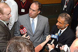 |
U.S. Rep. John Sweeney, center, and Albany NanoTech President Alain Kaloyeros, at right, speak with members of the media at the Albany Symposium. |
ALBANY, N.Y. (September 26, 2005) -- U.S. Rep. John Sweeney announced a partnership between IBM Corp., Applied Materials and Albany NanoTech to conduct advanced R&D in six areas that are essential to the development of future generations of computer nanochips. The announcement was made at the Albany Symposium, an annual gathering of semiconductor industry officials and academic researchers at the Sagamore resort in Bolton Landing on Lake George, New York.
Under the $300 million, five-year program, more than a 100 researchers and engineers from Applied Materials, IBM, and Albany NanoTech will work jointly at the complex to conduct research, beginning with the 32nm (1/3000 the width of a human hair) computer chip device node.
Other key R&D areas include leading edge nanomaterials such as 300mm epitaxial substrates and ultra-low k dielectrics; nanoscale process technologies including atomic layer deposition for liners and chemical mechanical polishing; and ultrafine ion implantation technology for nanoscale semiconductor devices.
Potential applications include real time visualization, three-dimensional holography, highly intuitive software for artificial intelligence, ultra-fast telecommunications, intelligent sensors for environment, energy, and homeland defense, nanobiochips for blood testing, DNA sequencing, and drug development and delivery, extremely powerful computing stations and servers, and smaller, lighter, and more efficient electronic devices of every kind.
"Hi-tech, high-paying jobs based on a sound science and education strategy are what we need for the knowledge-based economy of today and tomorrow," Congressman Sweeney said. "This $300 million partnership reminds us again that New York led by Albany Nanotech can compete and dominate the enabling hi-tech sectors of the global economy. I will continue to do everything that I can to support the essential world-class research and development programs that take place at Albany Nanotech."
"We're creating a high-end facility where private corporations can send researchers to undertake work that they would not otherwise be able to do," UAlbany President Kermit L. Hall said. "By creating a common research site we are strengthening the role of the university and Albany NanoTech as a center of collaborative and cooperative research."
"The semiconductor industry's challenges in further advancing IC (integrated circuitry) technology into the nanoscale regime requires an expanded scope of work on new materials, new processes and more," said Mark Pinto, Applied Materials (AMAT) senior vice president and technology officer. "These challenges demand more extensive joint development efforts among leading companies in the IC business -- companies such as IBM and Applied Materials. We are proud to partner with IBM at Albany Nanotech to foster this next wave of research and development that will lead to more powerful, more portable and more affordable chips. We also thank Congressman Sweeney for his support of this global high tech partnership."
John Kelly, IBM's senior vice president for technology and intellectual property, remarked, "The addition of advanced technology and research support from Applied Materials is an important milestone in establishing the IBM-Albany NanoTech Center for Semiconductor Research as the nation's premier facility for the study of nanotechnology. IBM is committed to collaborative innovation and will continue to work with leaders in government, education, and the private sector, as exemplified by Applied Materials and Albany NanoTech, to keep New York State at the forefront of semiconductor research and development."
"We are delighted with Congressman Sweeney's announcement that Applied Materials and IBM are entering into such an outstanding partnership with Albany NanoTech," said SUNY Acting Chancellor John R. Ryan. "We are also extremely grateful to our private sector partners for their unprecedented investment in our high technology programs. These investments are further proof that the State University of New York, in general, and the University at Albany, in particular, are leading the world in nanoscience and nanotechnology."
"The establishment of our partnership with the two giants of the nanoelectronics industry, Applied Materials and IBM, represents a critical enabling step in our strategic plan to establish Albany NanoTech as a global intellectual powerhouse," said Alain Kaloyeros, president of Albany NanoTech and vice president of UAlbany's College for Nanoscale Science and Engineering. "This partnership will significantly strengthen our research, educational, and workforce training programs, and our ability to better serve our industrial, defense, and academic customer base. We thank Congressman Sweeney for his vision and leadership in advocating such programs, particularly at the federal level, and welcome the Applied Materials and IBM researchers to the Albany NanoTech complex."
About Albany NanoTech
One of the largest global centers for nanotechnology,
Albany NanoTech is home to the College
of Nanoscale Science and Engineering
(CNSE) and the New York State Center
of Excellence in Nanoelectronics (NYSCEN)
of the University at Albany. The 450,000
square foot complex, with an asset value
approaching $2B, includes the only 200mm/300mm
wafer facilities in the academic world,
encompasses nanoelectronics, system-on-a-chip
technologies, biochips, optoelectronics
and photonics devices, closed-loop sensors
for monitoring, detection, and protection,
and ultra-high-speed communication components.
The complex is projected to expand to
over 650,000 square feet and an asset
value in excess of $3B by the end of
2007. With over 65,000 square feet of
Class 1 capable 300 mm wafer cleanrooms,
as well as on-site faculty and student
researchers, Albany NanoTech provides
corporate partners with a unique environment
to pioneer, develop, and test new nanoscience
and nanoengineering innovations within
a technically aggressive and financially
competitive R&D environment. For
more information, visit www.albanynanotech.org.