|
Campus News
Albany NanoTech and AMD Team Up
to Develop Breakthrough Silicon Measurement
Technique
by Shonna Keogan and Greta Petry
(December 10, 2004)
 |
|
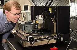
Robert Geer will supervise
Albany Nanotech's collaboration with Advanced
Micro Devices, the goal of which is to
find a method to measure stress levels
in strained silicon, the base material
in high-performance microchips.
|
Advanced Micro Devices (AMD) is targeted at
helping AMD find answers to some fundamental
research questions, according to Robert Geer,
associate professor of nanoscience at the University
at Albany�s new College of Nanoscale Science
and Engineering (CNSE).
The collaboration, announced November 9, represents
the first industrial partnership for the college.
The goal is to find a new method to measure
stress levels in strained silicon, the base
material in high-performance microchips. Geer
will supervise the project.
Straining silicon makes electrons flow more
quickly through transistors, enhancing performance
of semiconductors while reducing energy usage.
The new technique seeks to enable the stress
state in strained silicon to be measured with
a target spatial resolution better than 10 nanometers,
a critical capability for controlling and improving
the performance in semiconductor integrated
circuits (ICs).
The first developmental implementation for
nano-optical measurements will be assembled
at Albany NanoTech, which houses the CNSE.
AMD personnel from AMD-Saxony�s Materials
Analysis Laboratory in Dresden, Germany, will
participate directly in the research at Albany
NanoTech. Findings will be relayed directly
to the Dresden laboratory to characterize the
performance of transistors for future technology
nodes, which are expected to be manufactured
in AMD�s upcoming 300-millimeter computer chip
plant in Dresden.
�This type of research hinges on having the
right talent at the right facility, and Albany
NanoTech has that critical combination of infrastructure
and expertise,� said David Kyser, director of
external research, AMD Technology Development
in Sunnyvale, Calif. �By joining with Albany
NanoTech, we�ve found a cost-effective way to
stay on the cutting edge in this area of nanoscale
research.�
President of Albany NanoTech and Vice President
and Chief Administrative Officer of CNSE Alain
Kaloyeros said, �Our collaboration with AMD
is a perfect example of how leading companies
in the semiconductor industry are recognizing
the clear value proposition of Albany NanoTech,
which provides the benefit of our extensive
facilities while working with researchers on
the forefront of the field through the College
of Nanoscale Science and Engineering. We believe
this model is the perfect formula for enhancing
New York�s high-tech economy.�
Straining silicon compresses the atoms in
the crystal and is like �pushing billiard balls
more closely together,� said Geer, who added
that compressing the silicon crystal in the
transistor can make its electrons move 30 to
40 percent more quickly, resulting in a faster
transistor.
�One critical issue in nanotechnology is that
it is hard to measure how close the atoms are
to each other when you get to nano-sized structures,�
Geer said. �The mechanics just work differently
when one is measuring material that may be from
10 to 100 atoms in size.�
The project will focus on near-field nano-optical
techniques, exploiting the enhancement of the
optical field at a nanoprobe tip. �We are probing
areas that are smaller than the wavelength of
light,� Geer said. �So we need to use some tricks
to confine the light to these length scales.
Near-field nano-optics allows us to do this.�
This new technique would facilitate more accurate
stress measurements in high- performance chips,
helping chip manufacturers to reduce costs as
well as time to market for leading-edge microprocessors.
The most obvious application of strained silicon
is in building a faster chip.
�The first person to market with faster chips
will stand to make the most profit. So the people
at AMD want to get their new chips to market
as soon as possible. But the fundamental science
of this project, which centers on Raman spectroscopy,
can be broadly applied. For example, we are
working on other aspects of this technique with
Professor Igor Lednev of the Department of Chemistry,
who is an expert on Raman scattering,� said
Geer, noting that this is an example of the
interdisciplinary nature of CNSE, which opened
this fall.
Raman spectroscopy permits scientists to study
vibrations in molecules and crystals through
the interaction of light with the vibrations.
�Some of the energy of a photon sets off a quantum
of vibration, a phonon, in the material. Due
to energy conservation, the photon leaves with
less energy than it came with � its color is
shifted towards the red, or longer, wavelengths,�
notes The Optics Laboratory on the Web.
This slight change in color can be measured
to find the energy of the vibration in a molecule
or, in the case of crystalline silicon, to determine
the strain.
Geer noted that AMD-Saxony researchers were
at Albany NanoTech last year, and, more recently,
an AMD-Saxony engineer spent two months working
in the CNSE labs. �We are also planning to send
students to work in their labs in the very near
future,� he said.
Geer added there is much symmetry between
Dresden and Albany in that both are sites of
tremendous growth in the high-tech industry.
Dresden is the capital of the German state of
Saxony. The minister-president of Saxony, Dr.
Georg Milbradt, visited the CNSE in July of
this year. As a result of that visit, the CNSE
and the Technische Universität in Dresden
are working to formalize collaborations in various
areas of nanoelectronics and nanotechnology.
|
